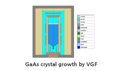
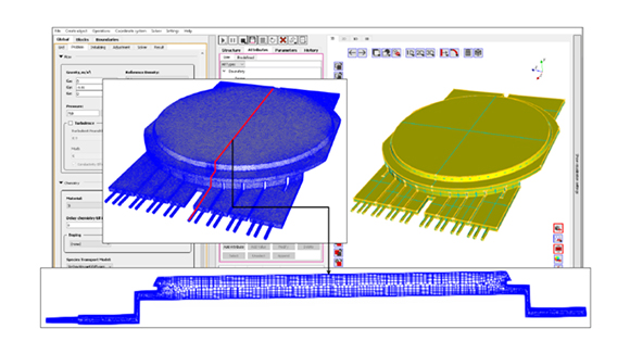
STR 시뮬레이션
CGSim
- Melt 또는 Solution으로부터 Crystal 성장 모델링 프로그램
● CGSim (Crystal Growth Simulator)
● Czochralski (Cz), Liquid Encapsulated Czochralski (LEC), Vapor Pressure Controlled Czochralski (VCz),
Bridgman growth 및 Kyropoulos (Ky) 공법에 대한 전문적인 시뮬레이션 S/W
● 적용되는 분야
- Hotzone 디자인 및 성장 조건을 조정하여 결정면의 형상과 V/G 분포를 제어하고 최적화할 수 있음
- 결정 품질을 유지하면서 결정화 속도를 높일 수 있는 조건을 찾을 수 있음
- 성장하는 결정의 stress 및 defect 제어 가능. Heat shield의 정확한 조정을 통한 defect engineering.
- 결정/도가니 회전 속도 및 다양한 강도 및 방향의 자기장을 통해 melt convection 제어 및 안정화 가능.
- Melt와 Gas의 불순물 이동을 분석함. Si Cz 성장에서 산소 및 탄소 함유 기체의 농도 예측 가능. 불순물
농도를 맞추기 위한 성장 조건을 조정하고 Hot zone의 최적 디자인 분석 가능
- 새로운 결정 성장 설정의 설계 및 최적화를 위한 모델링 지원
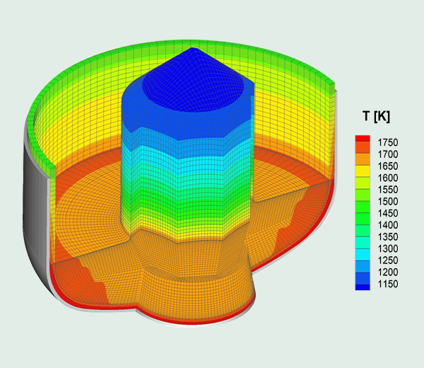
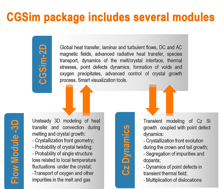
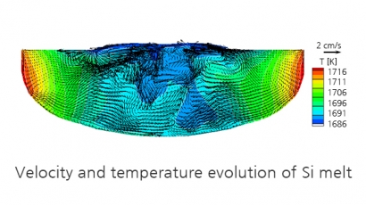
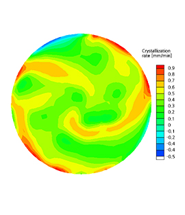
● CGSim은 2D Basic CGSim, 3D Flow Module, 그리고 Cz Dynamics로 구성되어 있음.
-
2D Basic CGSim
- Heat transfer
- Gas flow
- Melt flow
- Turbulence
- Melt/crystal interface shape
- Ready models for species (C, O, N, B, P)
- Thermal stresses
- Defects -
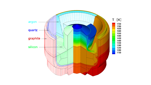
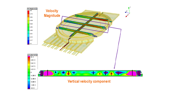
3D Flow Module
- Melt, Crystal, Crucible, Gas 영역 또는 Encapsulant 영역을 포함한
결정 성장의 3D 및 2D 난류(turbulence) 및 층류(laminar)의 대류를
전문적으로 분석하기 위한 S/W. 열 전달과 결합해서 분석하는
유일한 접근 방식이 사용됨.
- conductive heat transport, - laminar flow
- radiative heat transfer in semitransparent domains
- turbulent flow within the RANS, LES, or DNS approaches
- prediction of crystallization front shape
- magnetic field effect, - impurity transport
- stress computation, - scalar transport -
Cz Dynamics
- Cz Si 성장 과정의 transient modeling으로
Point defect 계산에 유용함 -
-

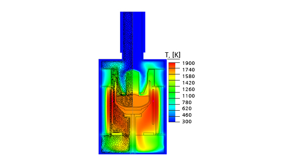
Virtual Reactor
- Virtual Reactor for Modeling of Epitaxy and Bulk Crystal Growth from the Vapor
● Vapor phase 에서 bulk crystal의 long term growth 및 epitaxy 를 시뮬레이션하기 위해 설계된 2D S/W
● 결정 성장 관련 현상을 분석하고, 성장에 따른 결정 형태의 변화를 모사할 수 있고, source evolution 및 defect dynamics 을 연구할 수 있음.
● 성장 시스템의 디자인과 공정 조건의 최적화와 단순화에 효과적으로 사용할 수 있음.
● 적용되는 분야 (For Bulk Crystal Growth)
- PVT SiC
- PVT AlN
- HVPE
- HTCVD of SiC
● 적용되는 분야 (For Epitaxy)
- III-Nitrides
- III-Vs
- CVD SiC
- CVD Si and SiGe
- HTCVD of SiC
- HVPE of III-Vs and Oxides
- MOCVD of Oxides
-

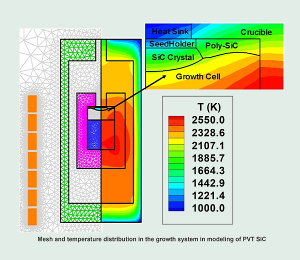
VR-PVT SiC
- Modeling of SiC Crystal Growth by PVT -
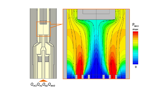
Modeling of HVPE (Nitrides, III/Vs, Oxides ) and MOCVD of Oxides
Schematic view of HVPE reactor, computed flow and ammonia partial pressure -
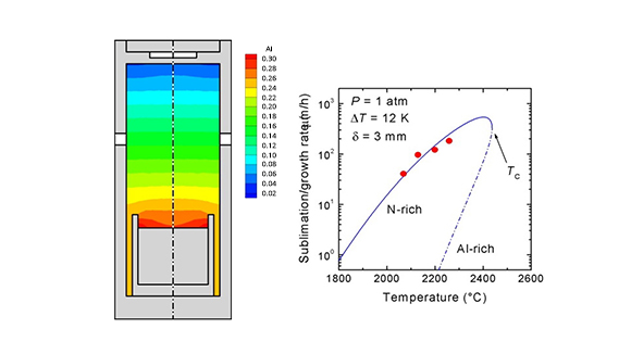
VR-PVT AlN
- Modeling of AlN Crystal Growth by PVT
Simulation of the species transport in an AlN growth system.
Left: Al distribution in the growth chamber. Right:
temperature dependence of the AlN growth rate -
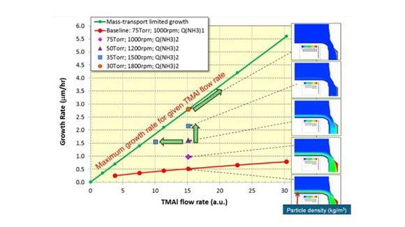
Modeling of the Epitaxy of III-Nitrides
-
Modeling of MOCVD of Si and SiGe
-
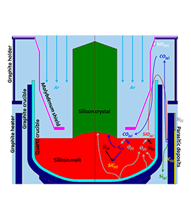
Modeling of SiC Crystal Growth by HTCVD
CVDSim 3D
- Software for 3D Modeling of CVD Processes
● Silicon expitaxy 및 SiC CVD 시뮬레이션을 위한 3D 모델링 소프트웨어
● CAD 도면 Import 기능, Grid 생성, 성장률 계산을 위한 물리적 및 화학적 모델, 모델링 결과 분석 및 시각화를 위한 도구가 포함되어 있음
● CVDSim 3D for Silicon epitaxy : Epitaxy 공정 시뮬레이션에 중요한 반투명 quartz의 열 흡수, 반사, 및 굴절 현상 및 forced와 natural convection의 중첩현상, 그리고 TCS 기반 Gas 혼합물의 화학반응을 계산함
● CVDSim 3D for CVD SiC : 다양한 유형의 reactor 에서 SiC epitaxy 모델링이 가능하며, SiC layer의 두께 균일성과 도핑 농도의 균일성을 분석하고 최적화하는데 사용될 수 있음
-
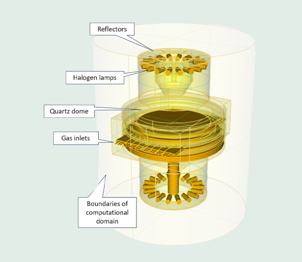
3D Global Heat Transfer model of Silicon Epitaxy
-
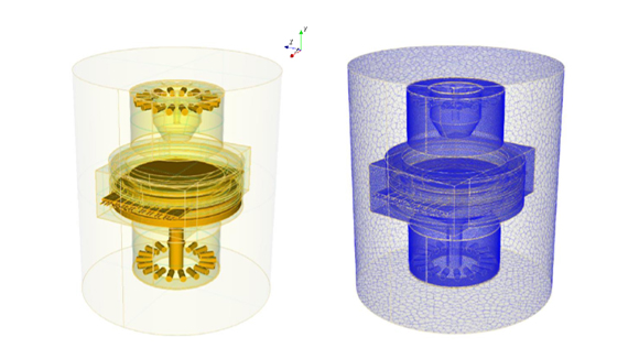
Flow Zone of Silicon Epitaxy
-
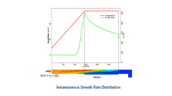
Simulation results of Silicon Epitaxy
-
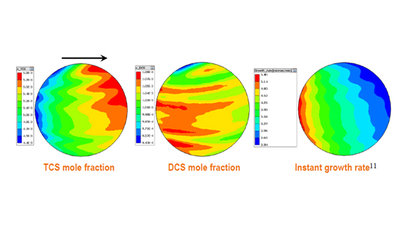
Simulation results of Silicon Epitaxy
-
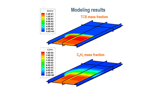
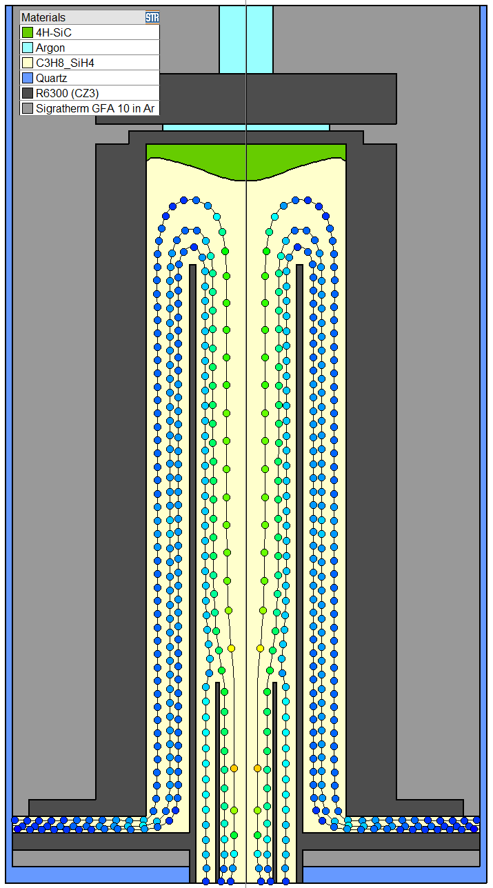
Simulation results of CVD SiC
-
Simulation results of CVD SiC
-
Simulation results of CVD SiC
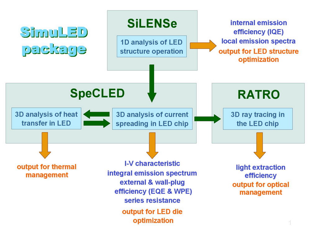
SimuLED
- 매우 빠른 웨이퍼 매크로 defect 검사 (장당 1초)
- 분석 표준 웨이퍼 사이즈: 50, 75, 100, 150, or 200 mm
- 분석 가능 particle 사이즈: 50 ~ 100 microns
- Brightfield, Darkfield, Oblique Lighting angles
- 조명을 변경하면서 연속적인 multiple scan 가능
- CSV 파일 또는 SECS/GEM compatible 파일로 데이터 자동 전송
● LED 및 LD 모델링 S/W로 III족 질화물 및 기타 wurtzite 재료 뿐만 아니라 hybrid 구조를 기반으로 하는 장치의 설계 및 최적화에 사용할 수 있음. 아래 영역에 대한 시뮬레이션이 가능함.
- carrier transport in the heterostructure and LED spectrum
- current spreading/crowding in LED die
- heat transfer in LED die
- light extraction from the LED die
● Drift-Diffusion 모델은 이종 구조의 캐리어 전송, 재결합 및 발광에 적용되는 반면, LED/LD die의 전류 확산은 3D hybrid 접근 방식을 사용하여 시뮬레이션이 됨. 이는 LED/LD에서 발생하는 필수적인 물리적 현상을 반영하면서 매우 빠른 계산을 가능하게 함.
● Die 의 자체 발열 및 전류 확산은 일관되게 자체적으로 시뮬레이션이 되며, 이는 high power 장치 및 Micro LED의 최적화에 특히 중요함.
● SimuLED package는 SiLENSe, SpeCLED 및 RATRO의 세 가지 호환 S/W로 구성됨.
-
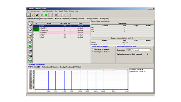
SiLENSe
- Cubic III-V 화합물(AlGaInAs, AlGaInP, InGaAsP, AlGaInSb 및 GaInAsSb)과
wurtzite III 질화물( AlInGaN 및 ZnMgO)로 제작된 LEDs 및 LDs 의 active region에
대한 1D Silmulation S/W.
- 프로그램에 탑재된 캐리어 전송 모델을 사용하여 극성, 반극성 및 비극성 구조를
시뮬레이션 할 수 있으며 polarization effects, high density of threading dislocations
및 Auger recombination 을 포함한 질화물 이종 구조의 특정 기능에 대한 모델링이 가능함.
- LED 이종 구조에 대한 부분(전자 및 정공) 전류, 전기장 및 전위, 캐리어 재결합 속도
및 캐리어 농도 등과 같은 중요한 요소에 대한 분포도의 결과를 제공함. -
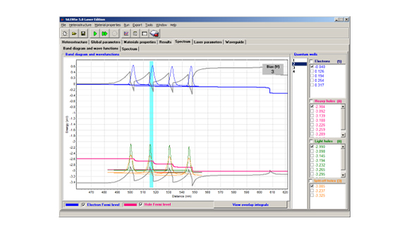
SiLENSe 시뮬레이션 결과
-
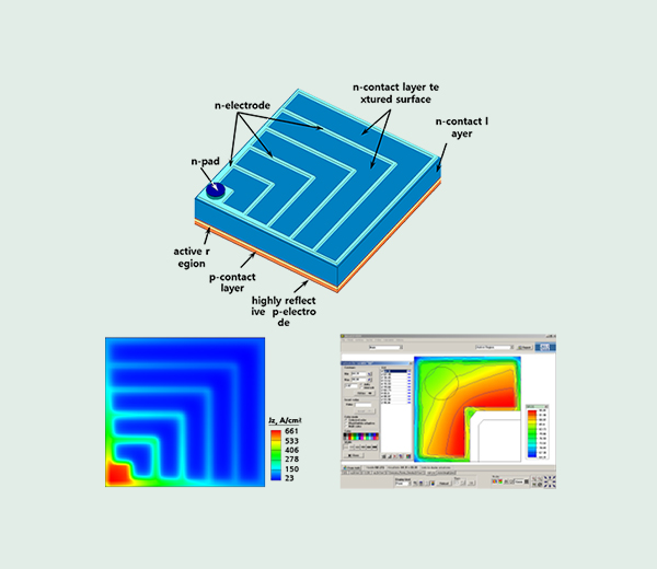
SpeCLED (Spreading of Current in Light-Emitting)
- planar 및 vertical LED chip의 전류 확산 및 열 전달을 모델링하기 위한 소프트웨어.
- 전류 밀도 분포, 내부 양자 효율(IQE) 및 활성 영역(active region)의 온도에 대한
시뮬레이션 가능.
- 순방향 전류에 대한 순방향 전압, output emission power 와 wall-plug efficiency
등과 같은 device의 여러 특성들을 계산합니다. -
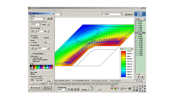
RATRO (RAy-TRacing SimulatOr of Light Propagation)
- LED chip 에서 광 추출(light extraction)을 모델링하기 위해 설계된 S/W
- 활성 영역(active region)으로부터의 광 전파(light propagation)와 흡수, 그리고
n- 및 p-contact layers와 wafer를 통한 LED die로부터의 추출(extraction)에 대한
광선 추적(ray-tracing) 시뮬레이션이 포함되어, 방출된 빛의 통합 추출 효율
(integral extraction efficiency)과 방사 패턴(radiation pattern)의 결과를 제공함. -
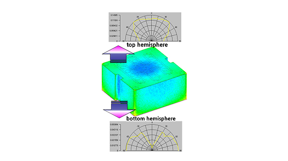
RATRO 시뮬레이션 결과
-
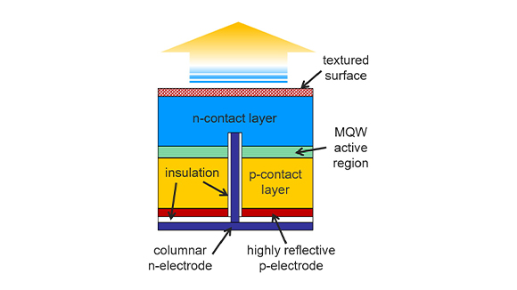
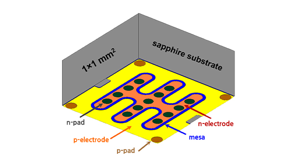
Micro-LEDs : Modeling of Surface Recombination and Light Extraction
-
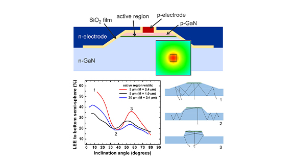
Micro-LEDs : Modeling of Surface Recombination and Light Extraction
FETIS / PVcell
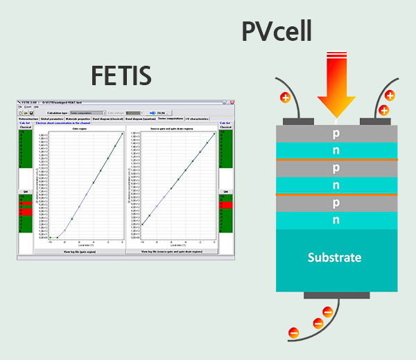
- FETIS:
- Field Effect Transistor Integrated Simulator – package for simulation of group-III nitride based high electron mobility transistors (HEMTs)
- Pvcell:
- Software for the Modeling of Semiconductor Solar Cells
● FETIS
- III족 질화물 기반의 high electron-mobility field-effect transistors (HEMTs)의 모델링을 위해 개발된 S/W
- Band diagram 과 device 이종구조 전반의 전위 분포에 대한 1D 시뮬레이션 S/W로서, 모델링의 결과에 대한 시각화를 제공하는 그래픽 셸이 포함되어 있음.
- Poisson 및 Schrodinger 방정식의 일관된 솔루션을 기반으로, HEMT 구조의 캐리어 confinement에 대한 준고전적 및 정확한 양자 역학적 고려 사항을 모두 사용하여 모델링을 함.
- 캐리어 농도 profile, sheet 캐리어 농도, 2D 전자/정공 gas subband의 개수 및 에너지 위치, 게이트 바이어스에 따른 변화 등의 HEMT의 중요한 특성들을 예측할 수 있음.
● PVcell
- 다양한 inorganic 반도체 재료로 만들어진 p-n 접합 및 tandem solar cell에 대한 빠르고 효율적인 1D 시뮬레이션 S/W이며, Si, Ge와 III-V binary 화합물 및 합금, 그리고 III-질화물 및 II-산화물 wurtzite 반도체 및 합금에 대한 Material database가 제공됨.
- 아래와 같은 영역에 대한 시뮬레이션이 가능함
1) Current density, power, conversion efficiency
2) Band diagram, electric potential, electric field
3) Carrier and ionized impurity concentrations
4) Generation rate, recombination rates (different channels)
5) Partial electron and hole current densities
-
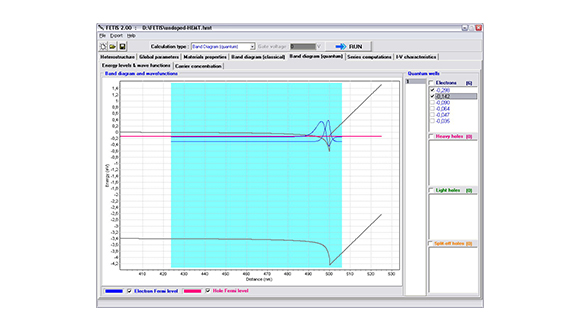
FETIS 시뮬레이션 결과
-
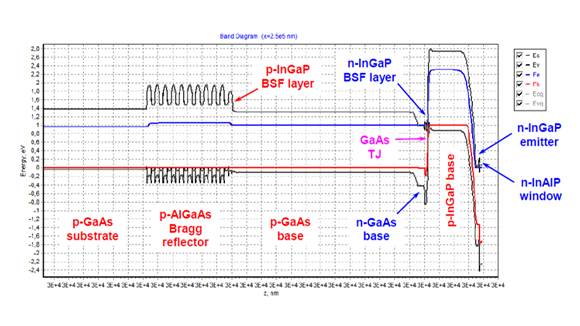
PVcell 시뮬레이션 결과
폴텍(주)
서울시 광진구 능동로3길 54 (태원빌딩 3층) 사업자 등록번호 : 206-86-48533 Tel. 02-418-5244 E-mail. sales@paultec.co.krCopyright (C) 폴텍(주). All rights reserved.Designed by WebSite.co.kr